
This is insane! I don't think I'd have it in me to make something like this! :)
A member registered Dec 15, 2022
Recent community posts
Hey! Thanks for your response.
Sorry about the confusing short-handed chip names!
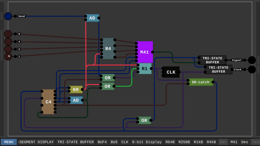
The "C4" Chip is a 4-bit counter I made.
The "M41" Chip is a Multiplexer that chooses from four inputs to be sent to one output.
As for sending my save, that's good to know! I'll attach the project file in this response after I give it a once-over. That way you can see how each chip was built!
I'd also like to show my modified clock, since it's kinda the heart of the serializer;
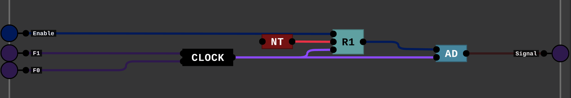
The base clock runs constantly. The enable signal gets written to the register on the next rising edge of the clock. The register output is AND-ed with the base clock output. This ensures the clock always has a consistent output when being enabled, as the enable signal can't make the output pulse prematurely.
The F0 and F1 signals control the frequency of the clock.
It's about time I started experimenting with serial encoding in DLS.
First things first, What's the difference between parallel and serial communication?
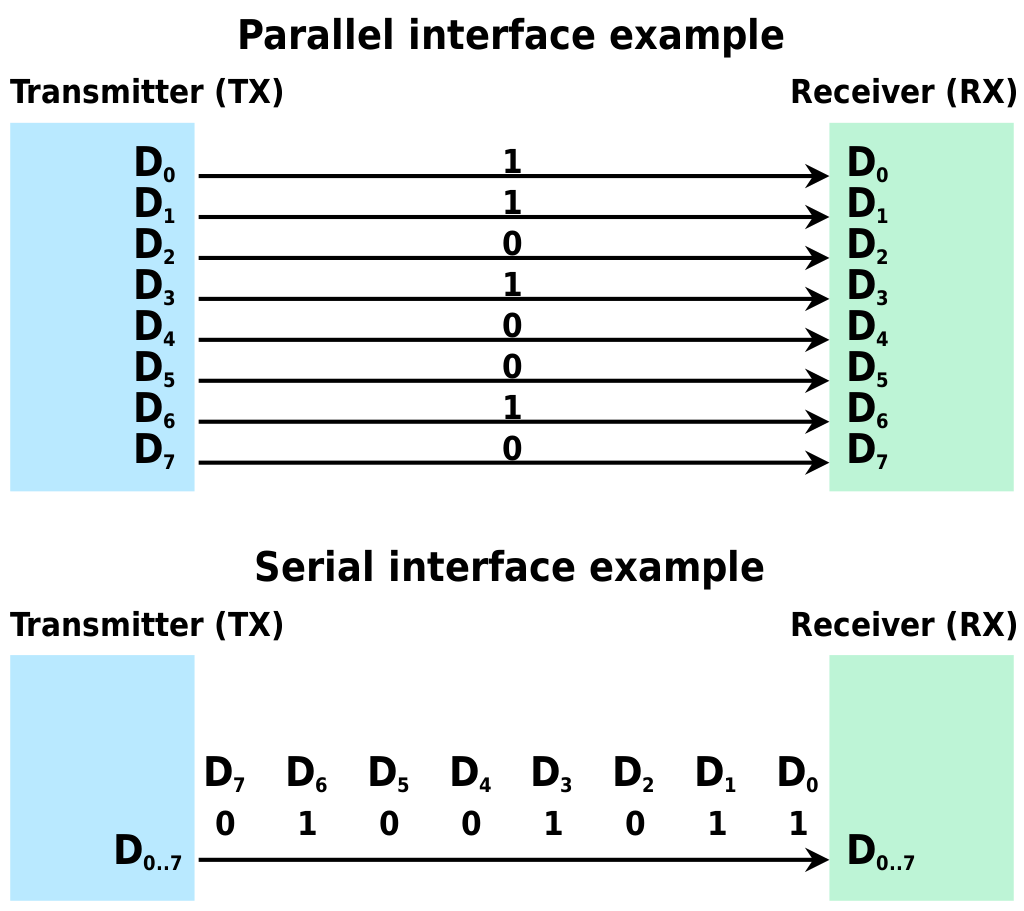
In Sebastian's amazing Digital Logic Sim YouTube series, all communication has been done in parallel. This is where we send a given amount of bits all at the same time on their own wires. For serial communication, we need to send those bits one after the other, over time, on a single wire.
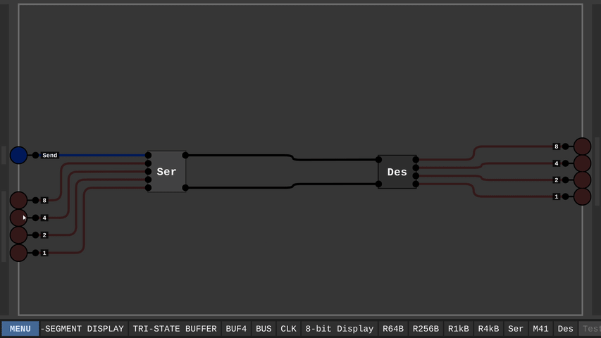
We'll need two chips to do this. A serializer, and a deserializer.
The serializer will take in a parallel binary input, and convert it into a series of pulses that represent the original number.
The deserializer will take in that series of pulses and convert it back into the original number.
So, in reality, at least for the way I went about this, the serial output will require two wires. one for the clock signal, and one for the data signal.
Here's how that would look;
Pretty neat, right? Don't worry, it get's very ugly from here! Boy, I really need to rework these things to be simpler, or at least look nicer.
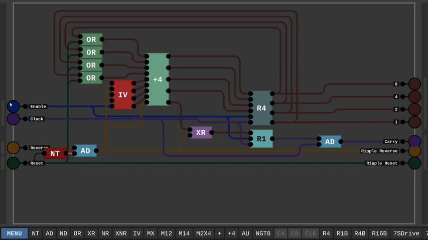
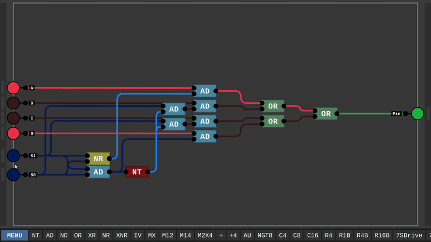
Alas, here are my first iterations of the serializer and deserializer;
Serializer:
Deserializer:
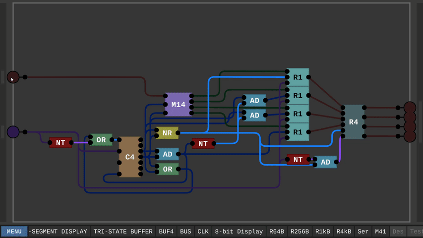
To be honest with you, I'm quite terrified to try and explain how these actually work. I'm almost certain there's a far better way to accomplish this behavior, but this is what I came up with.
Long story short, they both use a counter and multiplexor to select which bit is being written/read to/from a register. There is some logic to decide when the clock runs the counter, and some logic to decide when to write to the registers.
One concern for the future that I have, is that I've made the serializer with an internal clock. This may, or may not come back to haunt me later on.
And that's as much as I currently feel comfortable saying about these things!
I'll happily answer any questions you ask to the best of my ability!
This one took some time to get right, as I pretty much just built it from scratch using the diagram I showed as my guide. I'd love to hear your opinions on it! I'd also love to see someone come up with their own version and share it with me. I can't wait to experiment with creating more components that use serialized signals!
That's all for now! I've more DLS hijinks to get up to! Thanks for reading! <3
Digital Logic Sim community · Replied to Angus-Developer in My Journey with Memory in DLS - 1kB? No problemo :)
Hey, Angus! I decided to catch up with you! Have a look, yeah?
I've made an update to my registers using the new Bus lines. In short, it helped me greatly reduce the number of wires to be, well, wired!
I kept stacking and stacking using this design until, well, the simulator couldn't really take much more. I learned the hard way why you stopped at 4kB! :D
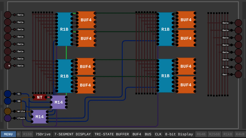
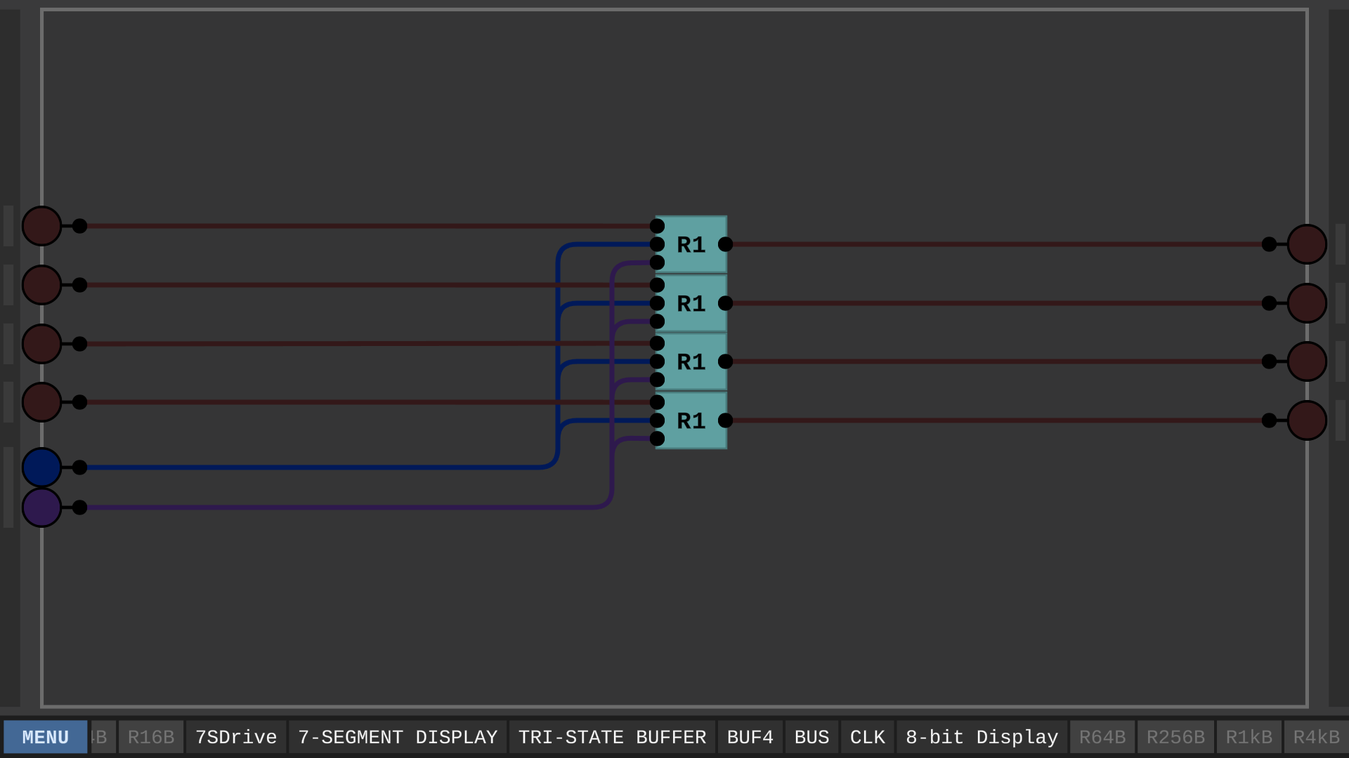
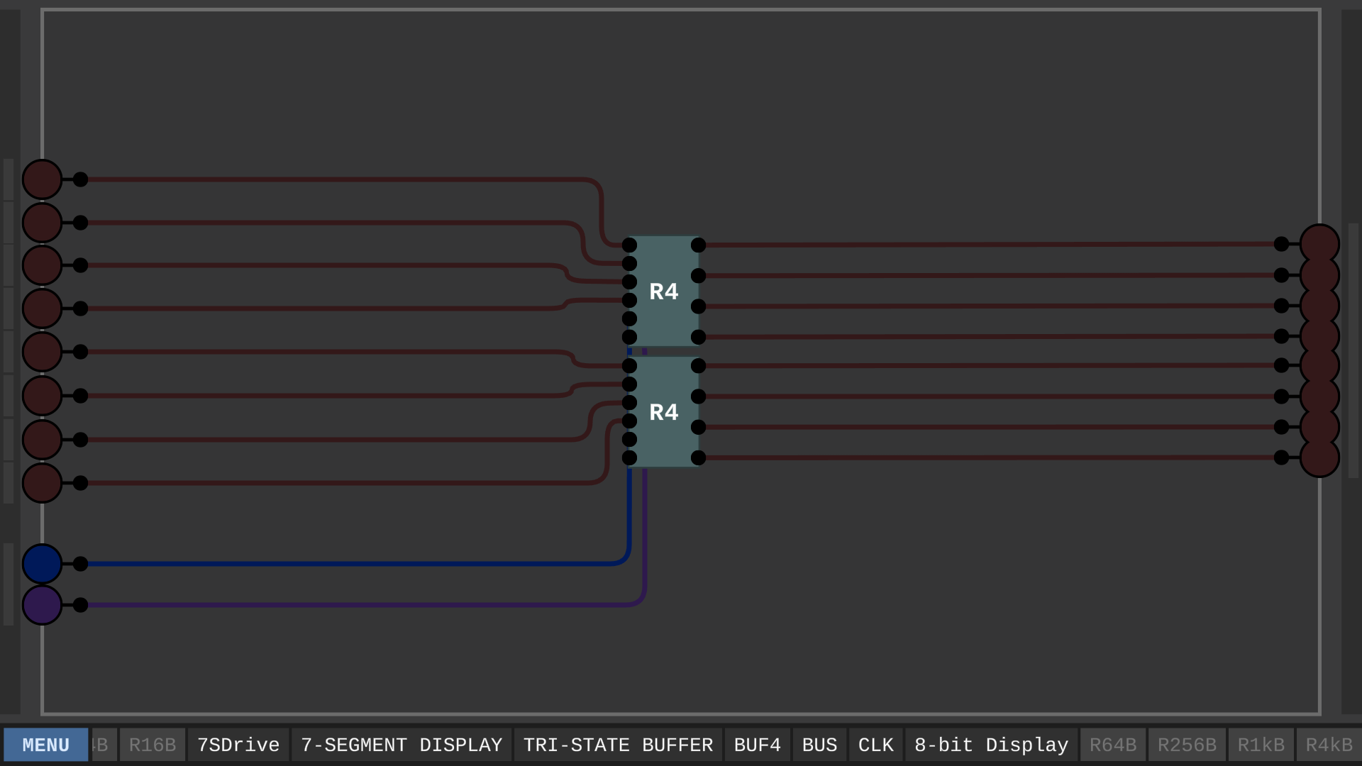
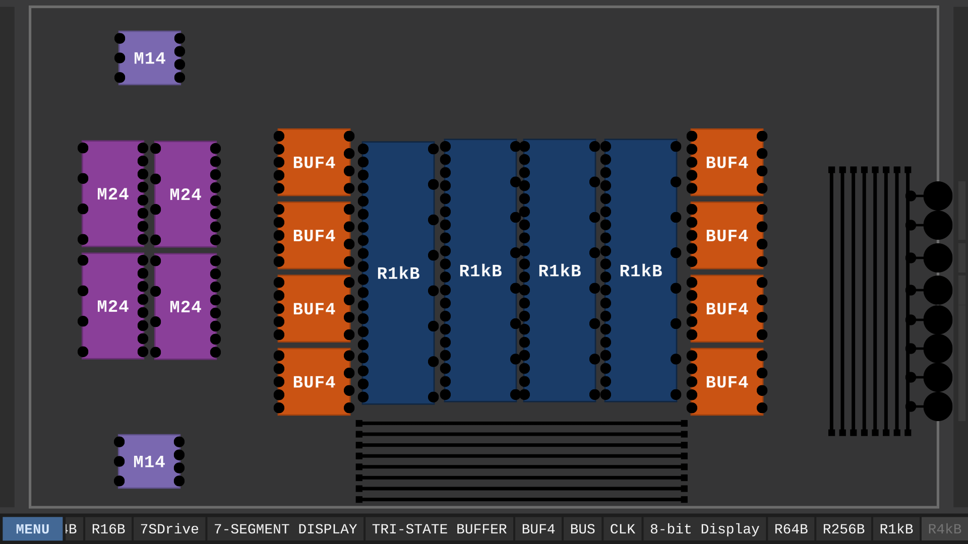
Let's start from the ground up, shall we? Here are all the registers I've built.

Here is what is inside each one of these, from left to right.....
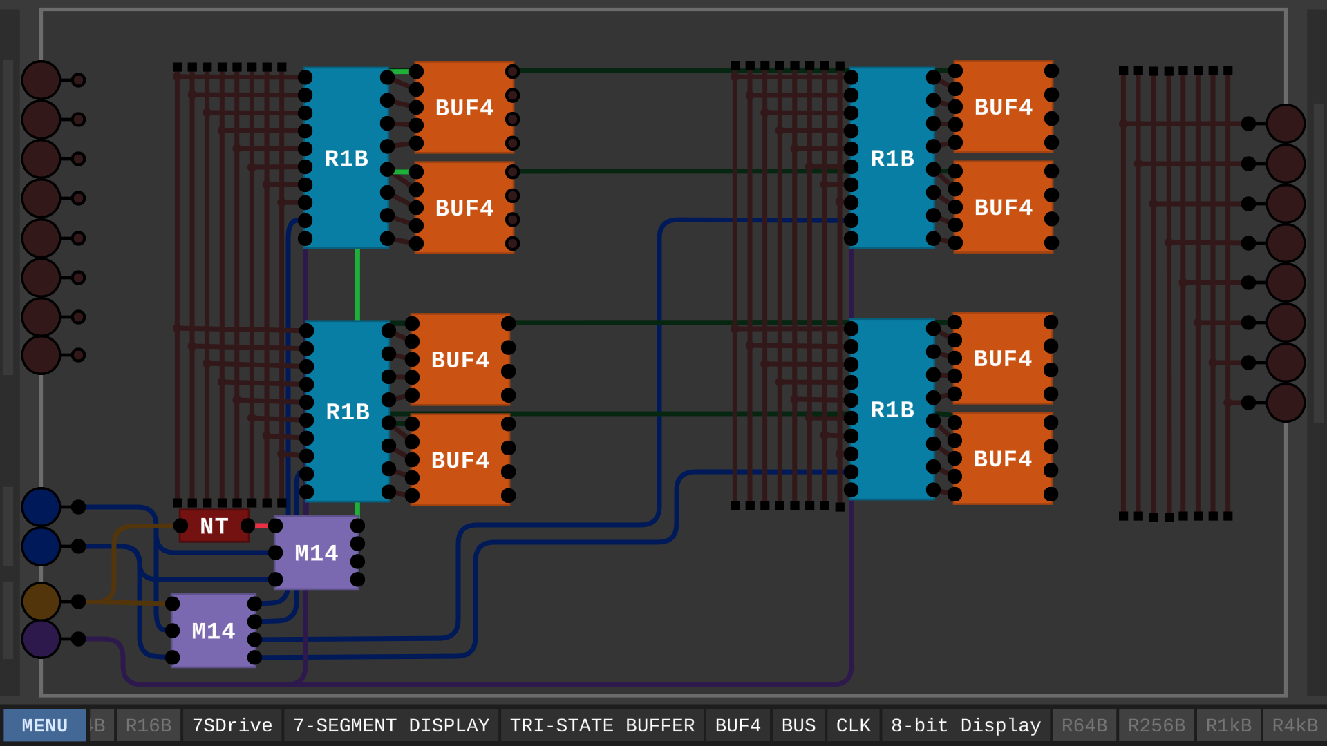
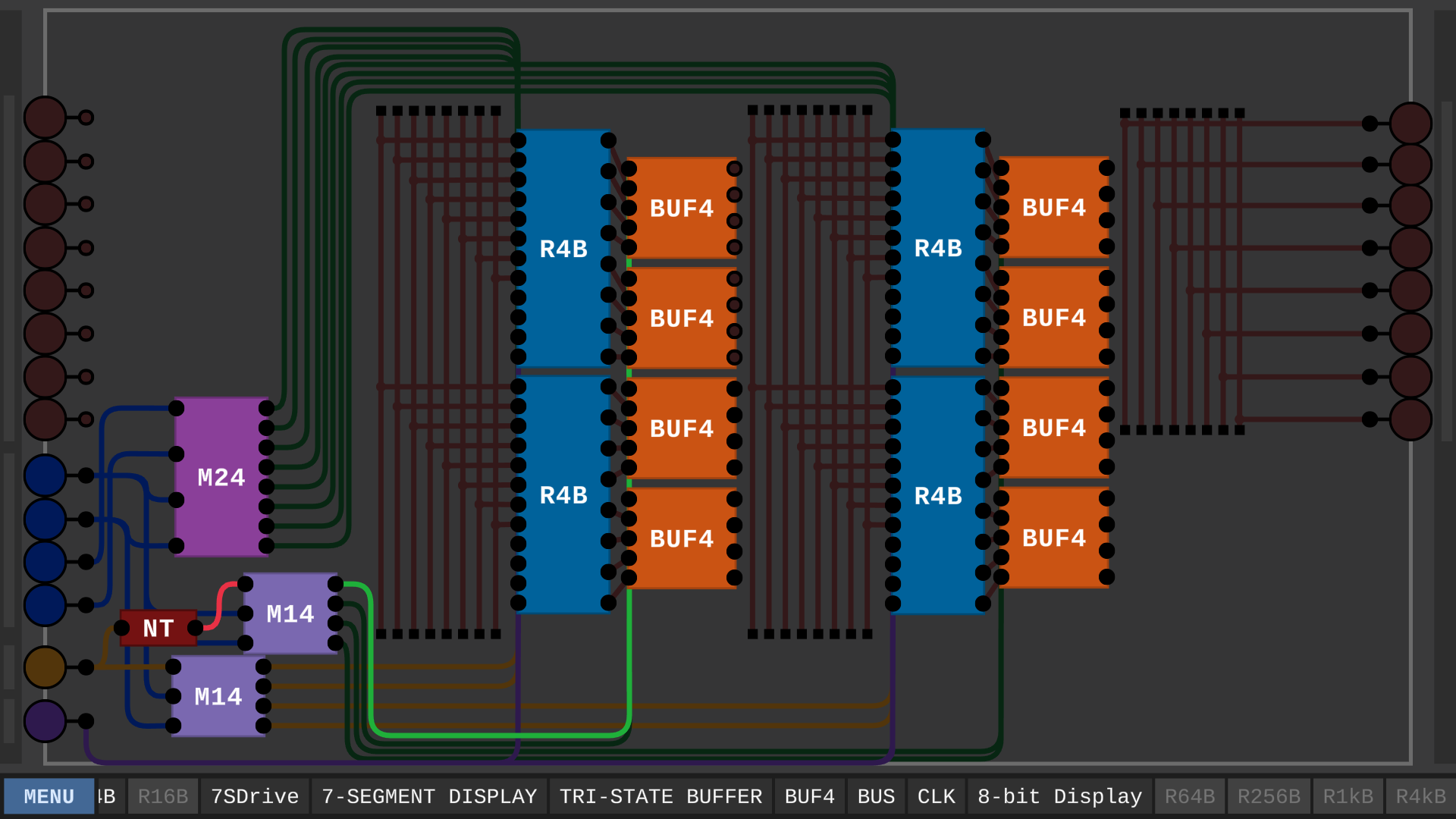
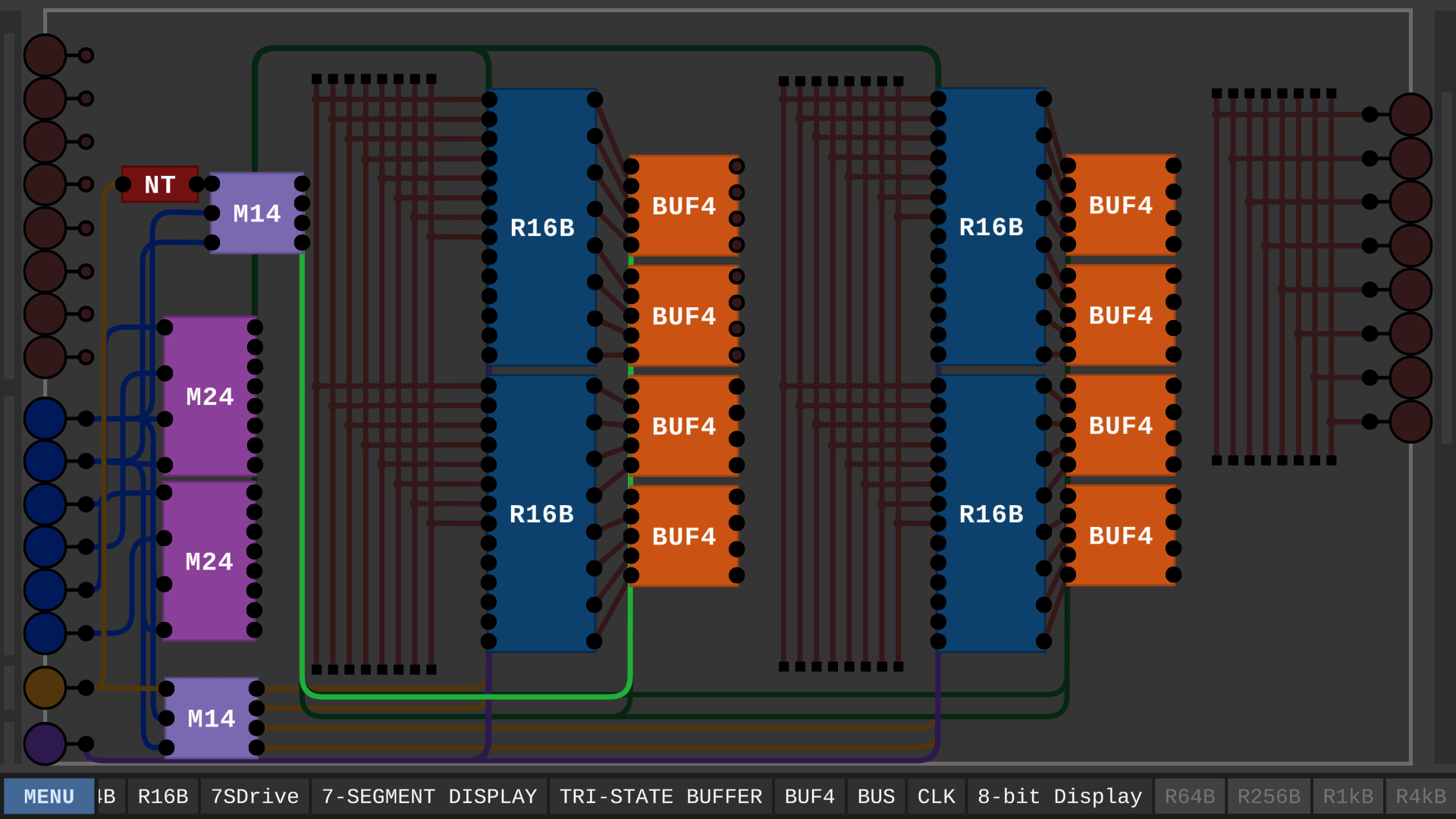
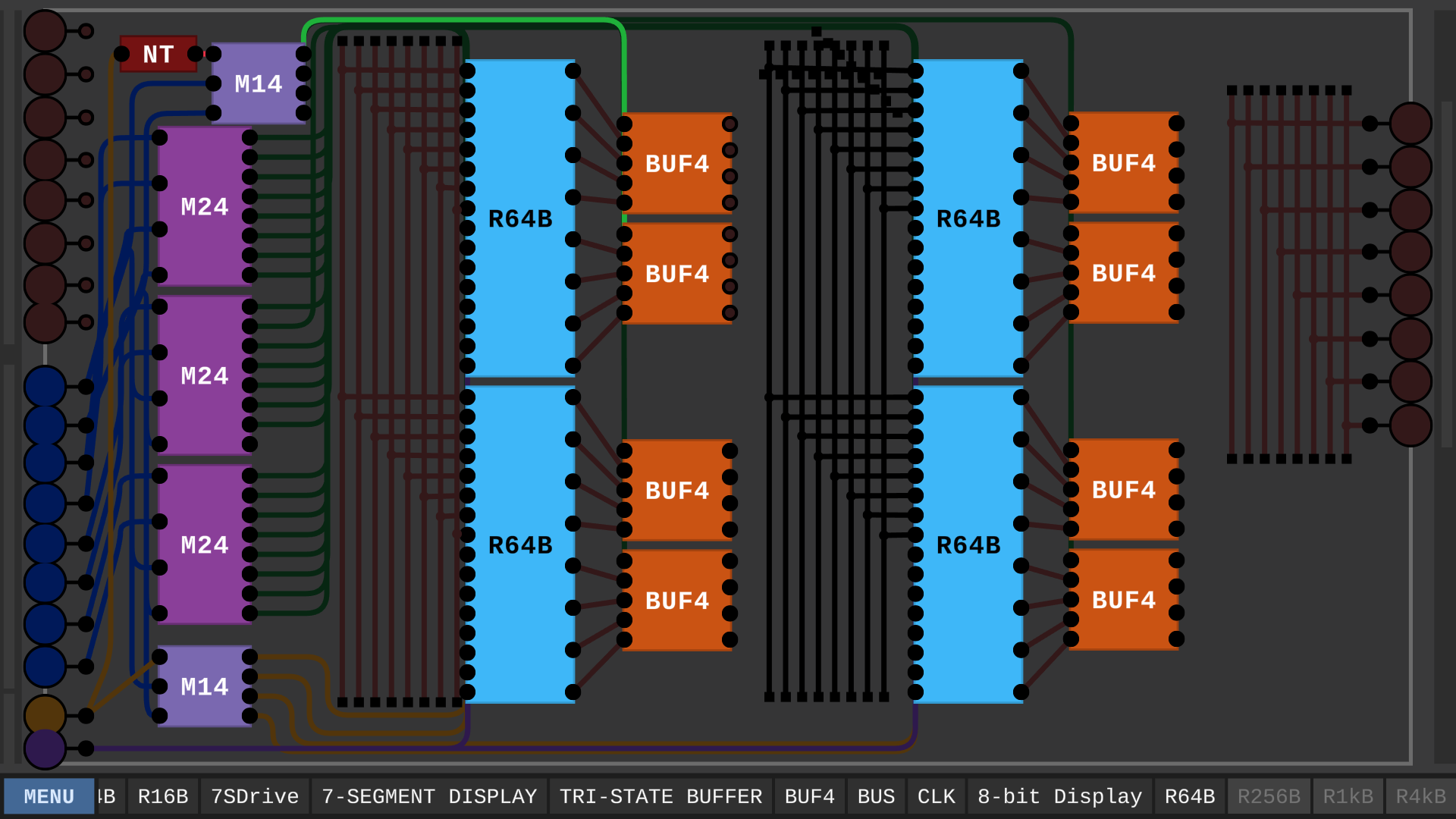
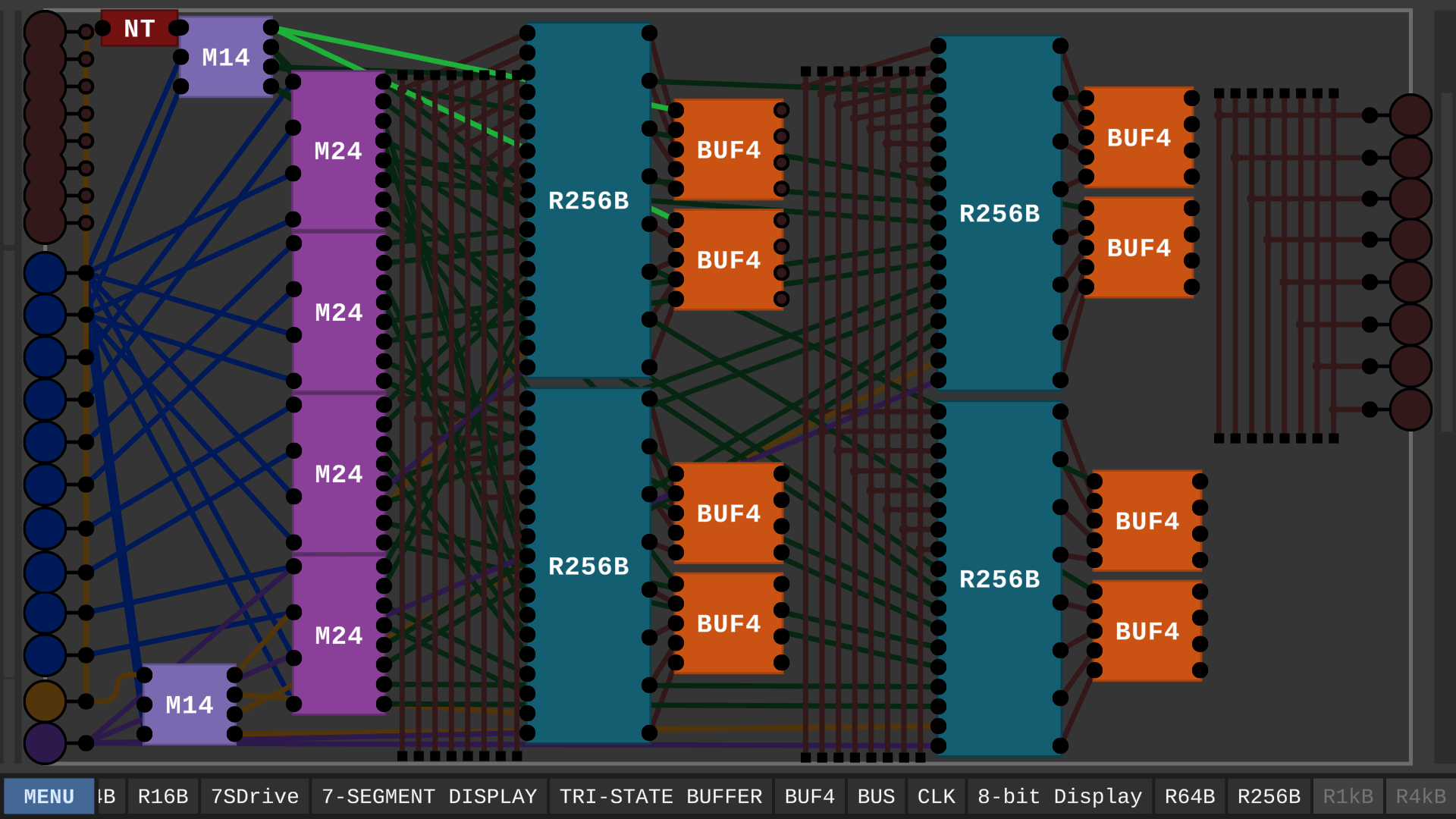
What a climb! As you can see, I got a little lazy with the wiring towards the end there.
This was also around the point where DLS's framerate began to give me flashbacks to Blighttown.
Because the simulator was running so slow, I couldn't be bothered to try and build 4kB, but I did set the chips down to conceptualize what it would look like. Not too much different, but I was beginning to run out of workspace, so I had to rearrange a few things;
If you ask me, 1kB is probably more storage than I'll ever need in DLS, so I'm happy with what I've made here.
Maybe when performance improvements are made I'll continue to stack this design.
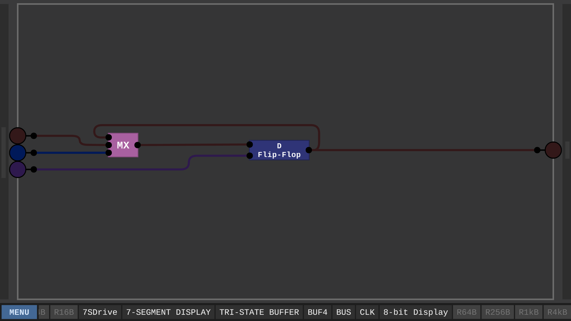
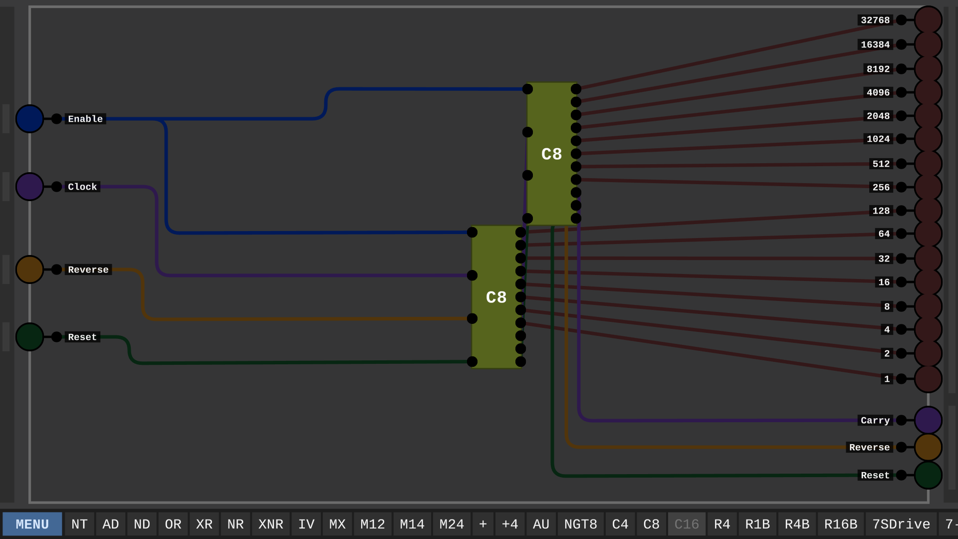
These aren't too terribly different from the register in my original post; They still use binary counting to select which byte is being read from / written to, but there is one main thing I'd like to point out, and get an opinion on.
If you take a look at the yellow pin, you'll notice it's connected to two small MUXs. One MUX has a Not gate behind it. It's the one connected to the Orange Bus Buffer chips. By doing this, I've made it so you can only either read or write to the chips at any given time. Turning the yellow Store, or, "Write" pin turns off the connection to the output pins. I'm not sure if this will be useful, but for some reason it seemed like the logical thing to do. (see what I did there? :p) I can, of course, always change it if needed.
I've also considered making a version that uses a counter to select the bytes, like a stack pointer or something? I've made one that has a toggle for counting in reverse, and so it would work. It would drastically reduce the amount of input pins needed, as you would only need the Data pins, Write pin, Clock pin, and reverse-counting toggle pin, and counter reset pin. Unfortunately, since the current version doesn't allow 7-Segment Displays to be embedded into chips, there would be no way to visualize which Byte is selected, without re-introducing all of the pins we just tried to bypass by adding the counter in the first place.
You could build a chip to convert a binary number into the same number of clock pulses, I imagine this would best be done using a multiplier, as it would require less pins than just inputting the Byte number you want to select. Having the reset pin can act as a sort of workaround to visualizing the selected byte, as you can just reset the stack pointer to 0 before moving it again.
The downside to the whole stack pointer Idea is that you can no longer select a Byte by sending bits in parallel; it has to be done with a given number of clock pulses. This means the read / Write time goes from nearly instantaneous to being dependent on where in the register you are writing to, because of the time it takes for the stack pointer to move there. Perhaps this feature would be better served in a serialized register, Which I also plan to make sometime.
Here's a 16-bit counter I made that would work well for this;
This counter doesn't slow down the simulation at all, and it can already select over sixty-five times the amount of Bytes I've managed to fit in a register. Although, because of the current maximum clock speed, it takes several minutes to count all the way up.
Here's the base counter that I stacked up to make this one; I think it may need a modification or two.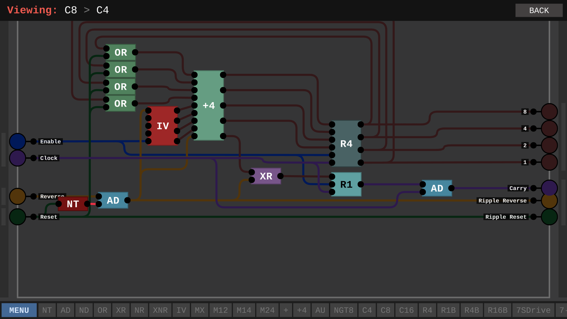
Because of the issues I mentioned, I think using a SerDes setup (Serializer - Deserializer) would work better than a counter. They could even be used together; We'll get there in a later post, but I have ideas.
(Side note; Inside the 256 Byte chip, you'll notice a bug I encountered where, if you screw up the bus line placement by only setting down pins, they cannot be deleted. Or, at least, I haven't yet found a way to do so.)